Ultra-clean sintered metal filter elements for process gas delivery, chemical mechanical polishing slurry, and cleanroom environment control — where a single metal particle above the critical dimension kills a chip yield target.
As semiconductor feature sizes shrink, the tolerance for particulate contamination also narrows. In process gas and DI water service, filter elements are selected for stable pore structure, clean surfaces, and low risk of media migration during operation.
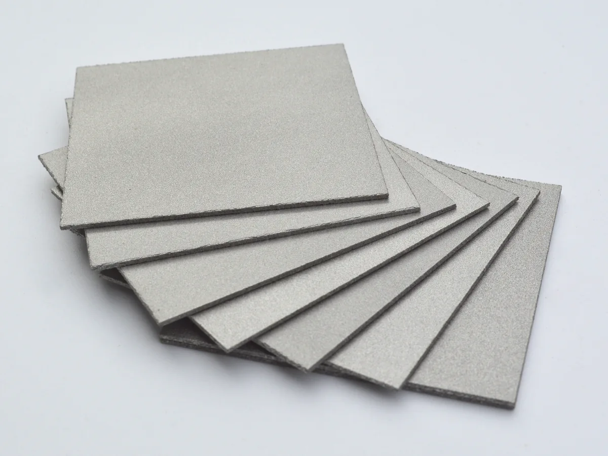
Sintered stainless steel filter elements address the particle cleanliness requirement. The sintered metal matrix is mechanically stable — no fibers, no binders, no migration risk. The solid sintered structure minimises surface area for particle adhesion compared with woven or fibrous media.
FILTURE supplies SS 316L sintered filter elements for semiconductor process gas delivery, chemical distribution, and CMP slurry filtration. For DI water polishing loops and gas diffusion applications, our sintered porous discs and tubes provide controlled distribution. Clean packaging and particle count testing are available on request for critical applications.
Housing dimensions are held to tight tolerances through post-sinter precision machining, and every batch can ship with particle count and material test reports for fab qualification records.
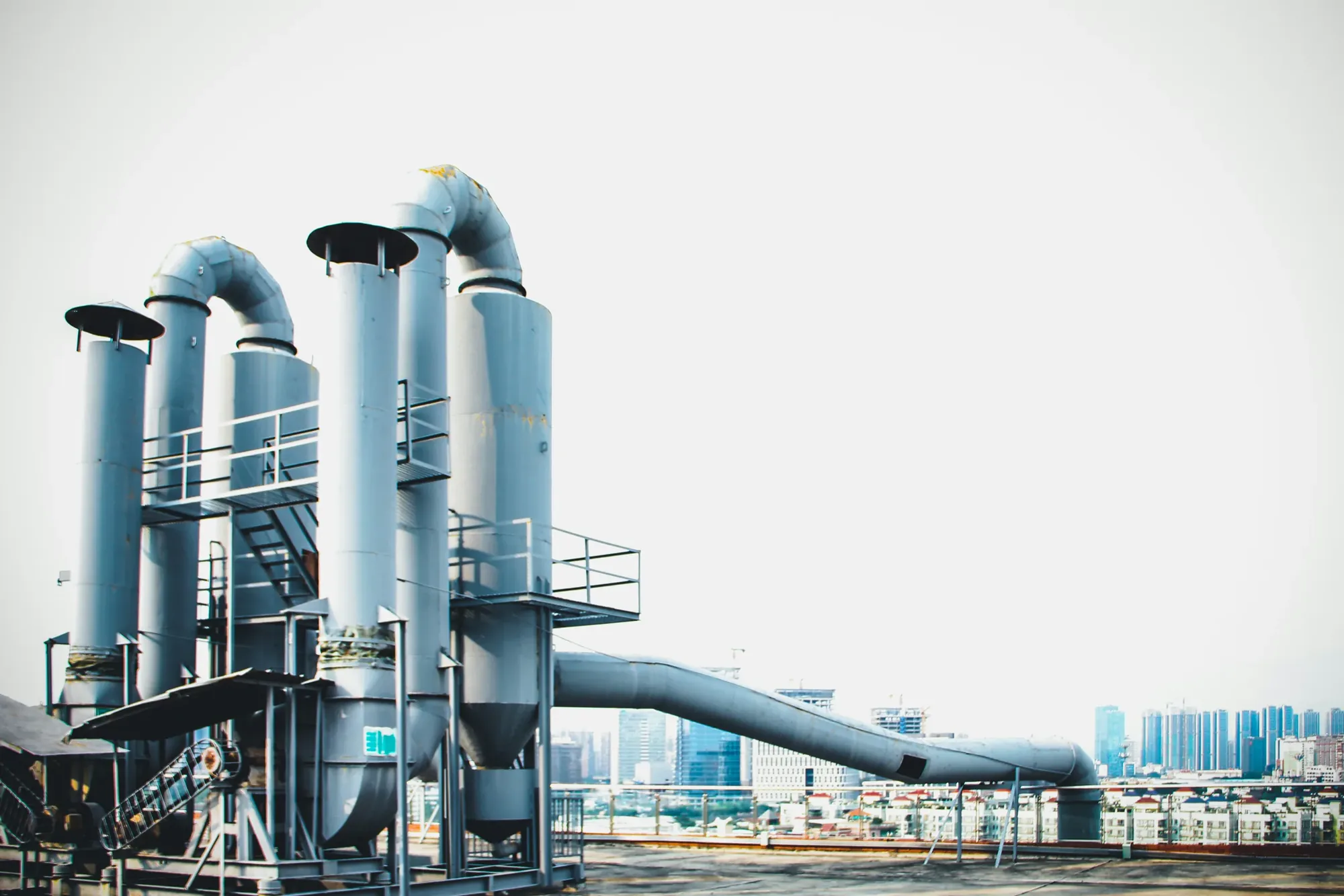
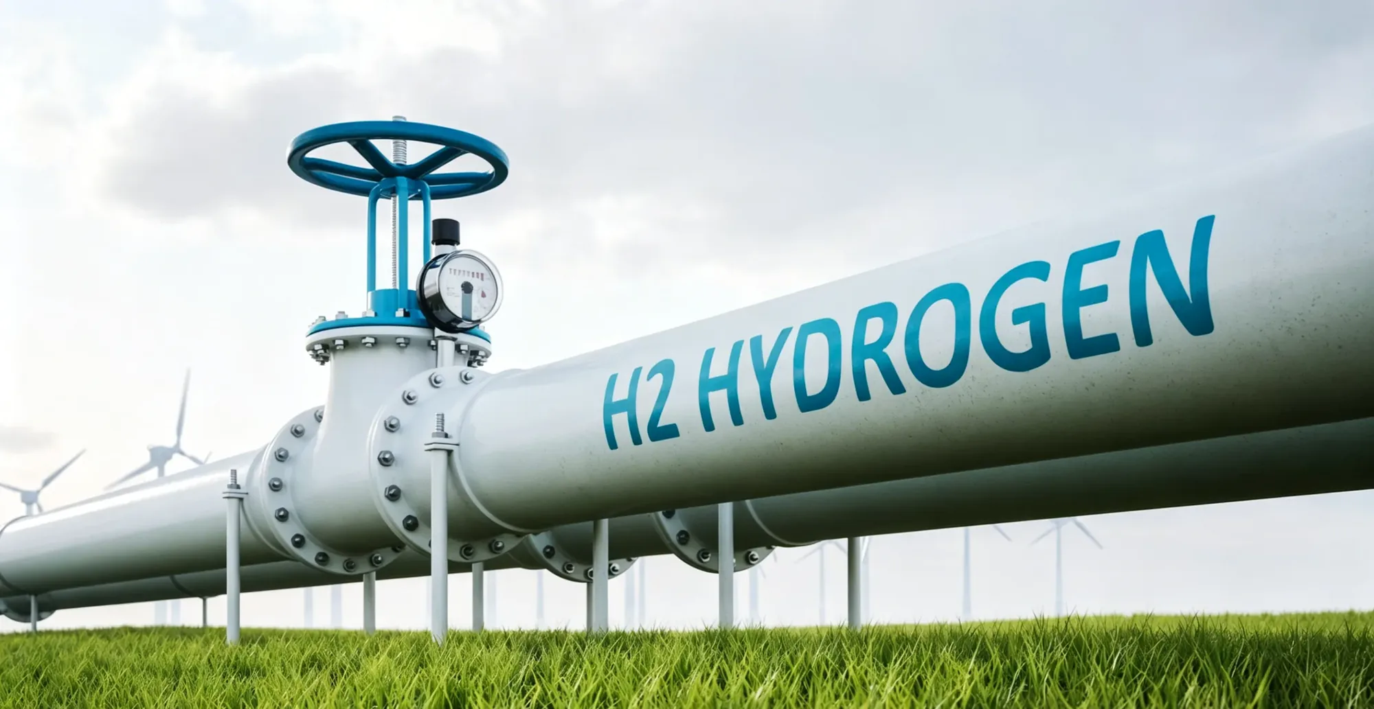
Sintered SS inline filters on N₂, Ar, H₂, and specialty gas distribution lines — a tightly-controlled pore size barrier limiting particles reaching process chambers, deposition tools, and etch systems.
0.5–5 µm · Low migration riskPoint-of-use filtration on chemical mechanical polishing slurry distribution — removing oversized abrasive particles before they reach the polishing pad and cause micro-scratch defects on wafer surfaces.
0.5–2 µm · Abrasion-resistant SSSintered SS filters on H₂O₂, HF, and other wet process chemical delivery systems — fine particle removal upstream of wafer wet-cleaning tools and etching baths.
1–5 µm · Chemical-resistant SS or TiMetal pre-filters on cleanroom HVAC and make-up air systems — protecting HEPA and ULPA filter banks from coarse particulate loading, extending final-filter service intervals.
5–50 µm · Stainless steel · Long lifeSintered SS elements as point-of-use filters on deionised water distribution loops — removing particles and bio-burden before water contacts wafer surfaces in cleaning and rinsing operations.
0.22–1 µm · DI-compatibleGas inlet sintered filters on diffusion and oxidation furnaces — maintaining ultra-pure N₂ and O₂ atmosphere in tube furnaces where any metallic contamination causes device leakage.
0.5–2 µm · High-purity · No outgassingControlled packaging options and particle count test reports are available on request for critical semiconductor applications.
Flat sintered plates for gas diffusion and distribution hardware, electrode substrates, and filter media blanks — cut to the dimensions of your process tool or chamber fixture.
View Details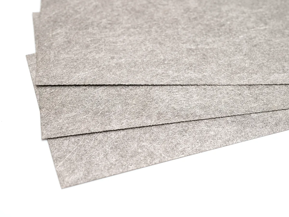
High-porosity sintered titanium fiber felt for specialty gas diffusion and filtration media in ultra-pure process gas lines, with low pressure drop at high flow rates.
View Details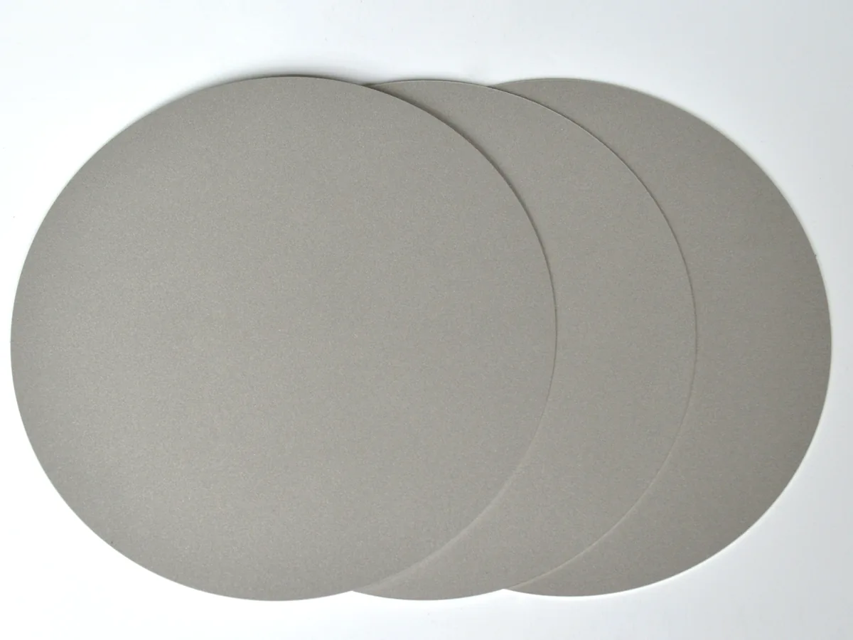
Sintered porous discs for gas sparging and uniform gas distribution in semiconductor process tools — providing bubble-free, laminar gas flow across the active process area.
View DetailsSintered SS is a solid, rigid structure with no loose fiber layers or binder resin in the filtration body. Compared with woven or polymer-based media, the sintered matrix is often selected where low particle release risk is important.
Sintered SS is a mechanically bonded solid matrix — no loose fibers, no binder resin, and no polymer layer in the filtration body. The metal matrix does not shed particles into the filtrate stream under normal operating conditions, pressure cycling, or thermal excursion.
Bubble distribution analysis is available on request, documenting pore-size distribution across the filter surface. Dimensional records and material certifications provided — semiconductor process engineers who need individual traceability can request the full documentation package.
"After installing FILTURE Ti porous discs in our DI water polishing loop, downstream cleanliness became more stable and easier to manage during the first several hundred hours of operation.
Fab Process Engineer Semiconductor Manufacturer · Taiwan
"We needed contamination-free filtration for a lithography process. The Ti element surface was verified with XRF — no detectable iron leaching. Cleanroom-compliant packaging made incoming inspection straightforward.
Cleanroom Engineer Fab Equipment Company · Japan
Share your gas type, operating pressure, pore size target, and surface cleanliness requirements. We'll confirm material grade, packaging options, and particle count testing availability.